Since the first developments of electrically powered technology in the mid-1800s, engineers, scientists, and manufacturers have created a diverse, multifaceted industry that fabricates millions of devices for a broad variety of purposes. Today’s massive demand for more and more intelligent designs and sustainable solutions functions in tandem with internationally standardized regulations in the industry. Not only are manufacturing practices and production facilities required to meet these industrial standards, but also the parts and assemblies themselves are standardized. This regimenting of basic components is beneficial to all manufacturing industries, not just electronics devices, and it’s created a production and distribution system that supports the work of original equipment manufacturers (OEMs) and contract manufacturers like us. MultiSource Manufacturing LLC provides semiconductor parts production and electromechanical assembly operations for several electronic device industries, including medical, defense, aerospace, and more.
SEMICONDUCTOR
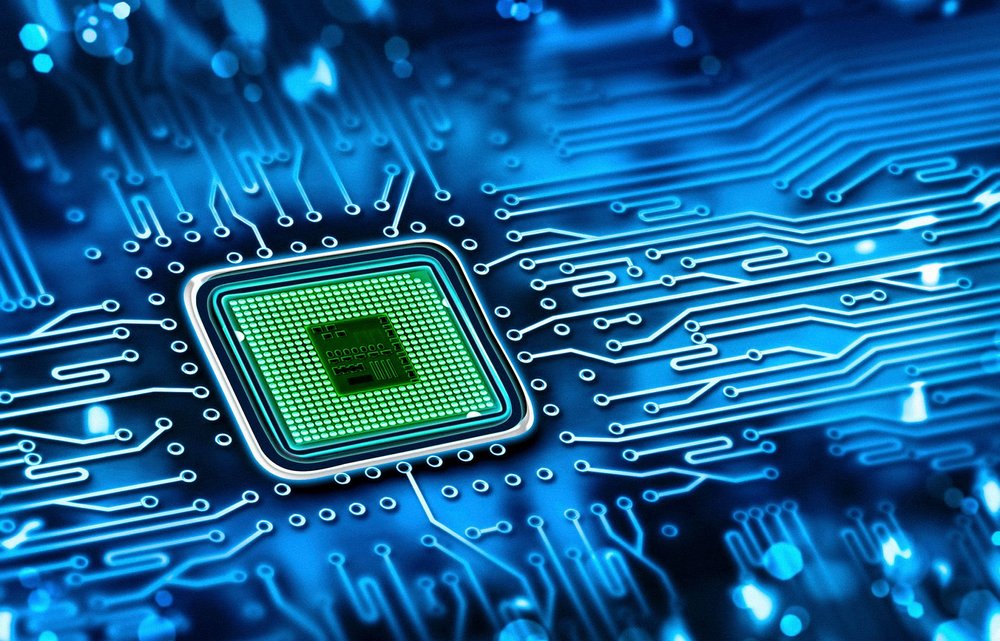
A critical part of the semiconductor and electronics production process is the fabrication and assembly of electrical packaging. Building the integrated circuit packaging used to encapsulate and work with the semiconductor microchip is another standardized process. We build high-quality packages that fit multiple current standards depending on the semiconductor and the application of the entire kit.
Earliest Circuit Packages
The earliest circuit packages were built in the 1960s. The first package was built in 1962 by Y. Tao, and it was the first version of ceramic flat packs, a packaging format that the U.S. military would use for several years. These ceramic packages are small and reliable designs.
The first integrated circuit package was developed in the 1970s. These designs also used ceramic as the main package material with all of the circuit leads along the same side of the chip. The first plastic package designs were dual in-line packages (DIP) that were developed in the late 1970s.
PIN GRID ARRAYS
By the 1980s, chips needed to grow to meet larger, smarter, and more intricate device specifications. This demand led to pin grid arrays (PGAs) and leadless chip carriers, in addition to surface mount packaging. These surface mount designs could take up to 30-50% less surface space with about 70% less thickness than DIP packages.
AREA ARRAY PACKAGES
In the early 1990s, the area array package was the next significant design development. This led to the popularizing of the ball grid array (BGA) and other array packaging techniques. Next, the plastic quad flat pack and thin small outline packages replaced PGAs for most devices.
FROM PGA TO LAND GRID
Industry leaders moved from PGA packages to land grid arrays in the 2000s, but most microprocessors still use PGA designs. BGA packages also grew into flip-chip ball grid arrays (FCBGA) that inverted the mounting of the die.
There have been several other recent packaging developments over the last 10 years, such as System in Package (SiP) and multi-chip modules (MCMs). MultiSource Manufacturing is capable of producing several types of packages with varying formats and materials.
SEMICONDUCTOR COMPONENTS
To learn more about our work with semiconductor components, contact us at (952) 456-5500. You can also request more information to get started with us today.