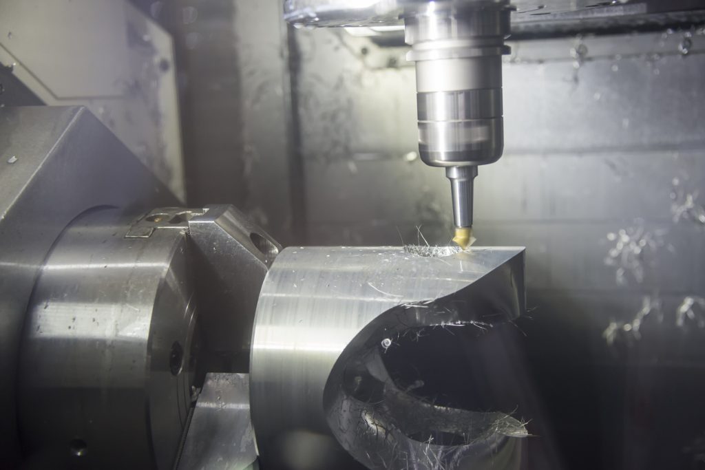
CNC Milling
CNC machining services produce consistent and precise components. Learn more about the quality CNC milling services from MultiSource here.
Learn MoreAt MultiSource Manufacturing, our customers come to us with their toughest challenges — and we deliver with innovative precision machining solutions and unparalleled support.

For over 50 years, MultiSource Manufacturing has provided customers with precision machining excellence. We specialize in tight tolerance components for the aerospace and defense industries.
With our innovative technology and high-quality processes, we are prepared to offer exceptional precision machining services, including CNC milling, CNC turning, Swiss machining, wire EDM services, and other secondary processes, like deburring. We understand that your parts may be used in critical applications so we are committed to ensuring your components match your precise requirements.
CNC machining services produce consistent and precise components. Learn more about the quality CNC milling services from MultiSource here.
Learn More
At MultiSource Manufacturing, we offer a variety of exceptional precision CNC machining services, including CNC turning. Learn more here.
Learn More
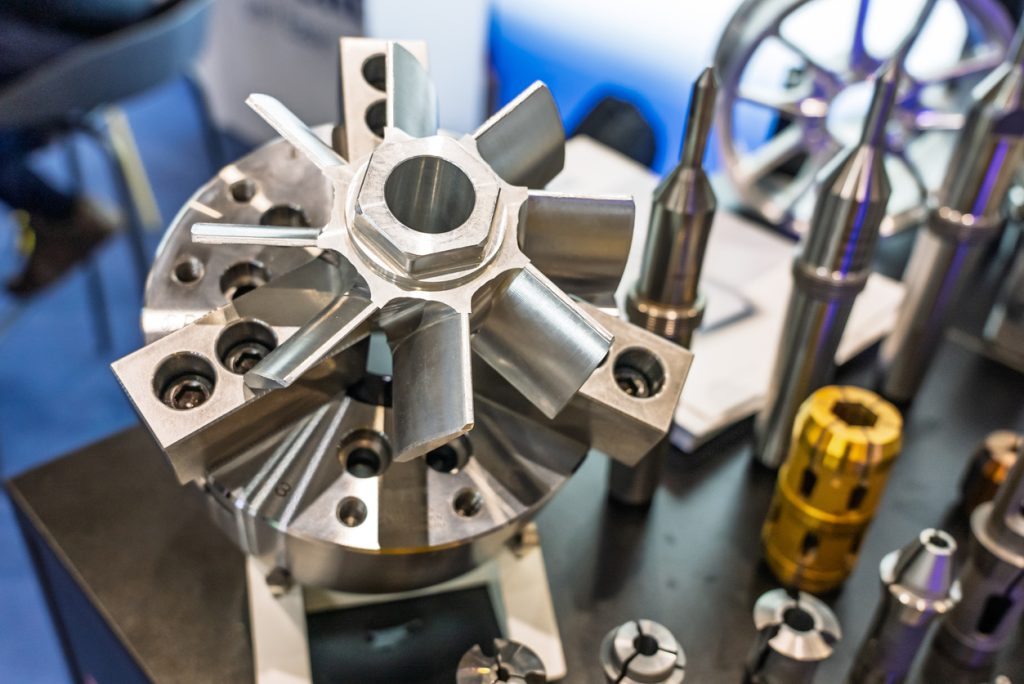
Trust our Swiss Machining services for small, intricate parts that require tight tolerances. We are capable of producing complex and accurate parts for a wide range of applications, and our state-of-the-art automated equipment allows for more efficiency during production.
Learn More
Our Wire EDM services are capable of producing parts with tight tolerances, sharp corners, and deep profiles. With our equipment and skilled team, our Wire EDM services enable us to produce versatile parts with a variety of materials and applications.
Learn More
At MultiSource, we offer both mechanical and electro-mechanical assembly. Our expert team and advanced automated technology allows us to finish your part to your exact specifications.
Learn More
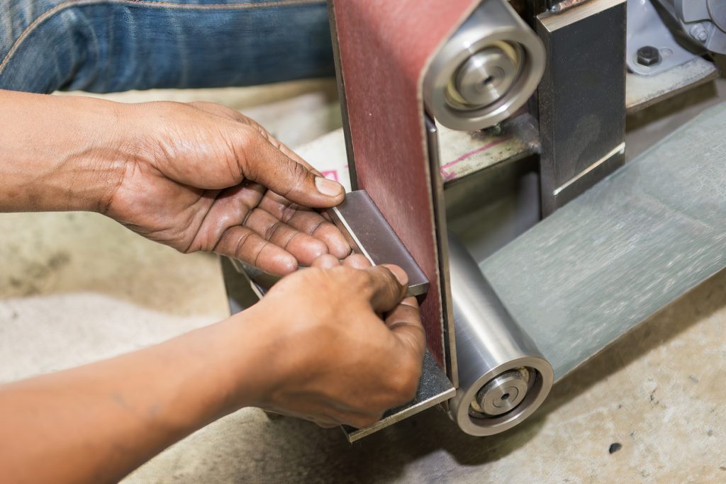
In addition to our precision machining services, we also offer value-added secondary services, such as heat treating, anodizing, passivating, welding, lasering, and painting through our expert sub-tier suppliers. We also offer inspection and inventory management services to further help you maximize value.
Learn More
MultiSource is skilled at providing accurate complex grinding services. Our CNC Inner Diameter and Outer Diameter grinding produce parts with very exacting tolerances, and we also offer other metal part fine finishing services, like honing and lapping.
Learn More
We are well-equipped to provide you with quality metal fine finishing services that will bring your fully-realized vision to life. With our collaborative approach, your part will exceed expectations.
We take pride in providing our customers with high-quality products. That’s why we are so adamant about adhering to industry standards. We are ISO 9001:2015, ISO-13485:2016, and AS 9100D-certified, and we also follow a strong cybersecurity compliance program. In addition, we are NIST 800-171-compliant and follow DFARS and ITAR requirements. You can have peace of mind knowing that your parts will adhere to all industry standards.

MultiSource has extensive experience serving the aerospace and defense, medical, semiconductor, and industrial markets. We understand the importance of adhering to industry standards, and with our comprehensive sub-tier supplier relationships and expert precision machining services, we are able to streamline production so you can stay competitive.
Tight tolerance machining can improve the overall function of your precision machined component. Explore more benefits here.
Poor accuracy in precision metal machining can result in equipment failure and unnecessary costs. Learn why precision matters here.
Deburring services can enhance part performance and result in a higher quality product. Learn more about the benefits here.